|
|
楼主 |
发表于 2013-5-21 19:18:54
|
显示全部楼层
An Example Hardwired CPU
1 Introduction- In this week's tutorial we are going to look at a simple hardwired CPU, to demonstrate that the control logic in a CPU can be built using some simple gates and multiplexors.
- The example CPU is one that I designed and implemented in Logisim over about a week at the end of 2010. The goal was to create a reasonably traditional architecture but with as little control logic as possible.
2 Architecture- The CPU has an 8-bit data bus and an 8-bit address bus, so it can only support 256 bytes of memory to hold both instructions and data.
- Internally, there are four 8-bit registers, R0 to R3, plus an Instruction Register, the Program Counter, and an 8-bit register which holds immediate values.
- The ALU is the same one that we designed last week. It performs the four operations AND, OR, ADD and SUB on two 8-bit values, and supports signed ADDs and SUBs.
- The CPU is a load/store architecture: data has to be brought into registers for manipulation, as the ALU only reads from and writes back to the registers.
- The ALU operations have two operands: one register is a source register, and the second register is both source and destination register, i.e. destination register = destination register OP source register.
- All the jump operations perform absolute jumps; there are no PC-relative branches. There are conditional jumps based on the zeroness or negativity of the destination register, as well as a "jump always" instruction.
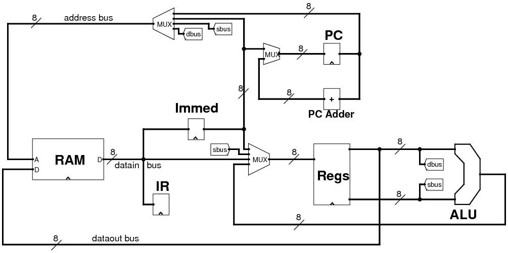
- The following diagram shows the datapaths in the CPU:
- The dbus and sbus labels indicate the lines coming out from the register file which hold the value of the destination and source registers.
- Note the data loop involving the registers and the ALU, whose output can only go back into a register.
- The dataout bus is only connected to the dbus line, so the only value which can be written to memory is the destination register.
- Also note that there are only 3 multiplexors:
- the address bus multiplexor can get a memory address from the PC, the immediate register (for direct addressing), or from the source or destination registers (for register indirect addressing).
- the PC multiplexor either lets the PC increment, or jump to the value in the immediate register.
- the multiplexor in front of the registers determines where a register write comes from: the ALU, the immediate register, another register or the data bus.
3 Instruction Set- Half of the instructions in the instruction set fit into one byte:
- These instructions are identified by a 0 in the most-significant bit in the instruction, i.e. op1 = 0X.
- The 4 bits of opcode are split into op1 and op2: more details soon.
- Rd is the destination register, and Rs is the source register.
- The other half of the instruction set are two-byte instructions. The first byte has the same format as above, and it is followed by an 8-bit constant or immediate value:
| op1 | op2 | Rd | Rs | immediate | | 2 | 2 | 2 | 2 | 8 |
- These two-byte instructions are identified by a 1 in the most-significant bit in the instruction, i.e. op1 = 1X.
- With 4 operation bits, there are 16 instructions:
| op1 | op2 | Mnemonic | Purpose | | | 00 | 00 | AND Rd, Rs | Rd = Rd AND Rs | | 00 | 01 | OR Rd, Rs | Rd = Rd OR Rs | | 00 | 10 | ADD Rd, Rs | Rd = Rd + Rs | | 00 | 11 | SUB Rd, Rs | Rd = Rd - Rs | | 01 | 00 | LW Rd, (Rs) | Rd = Mem[Rs] | | 01 | 01 | SW Rd, (Rs) | Mem[Rs] = Rd | | 01 | 10 | MOV Rd, Rs | Rd = Rs | | 01 | 11 | NOP | Do nothing | | 10 | 00 | JEQ Rd, immed | PC = immed if Rd == 0 | | 10 | 01 | JNE Rd, immed | PC = immed if Rd != 0 | | 10 | 10 | JGT Rd, immed | PC = immed if Rd > 0 | | 10 | 11 | JLT Rd, immed | PC = immed if Rd < 0 | | 11 | 00 | LW Rd, immed | Rd = Mem[immed] | | 11 | 01 | SW Rd, immed | Mem[immed] = Rd | | 11 | 10 | LI Rd, immed | Rd = immed | | 11 | 11 | JMP immed | PC = immed |
- Note the regularity of the ALU operations and the jump operations: we can feed the op2 bits directly into the ALU, and use op2 to control the branch decision.
- The rest of the instruction set is less regular, which will require special decoding for certain of the 16 instructions.
4 Instruction Phases- The CPU internally has three phases for the execution of each instruction.
- On phase 0, the instruction is fetched from memory and stored in the Instruction Register.
- On phase 1, if the fetched instruction is a two-byte instruction, the second byte is fetched from memory and stored in the Immediate Register. For one-byte instructions, nothing occurs in phase 1.
- On phase 2, everything else is done as required, which can include:
- an ALU operation, reading from two registers.
- a jump decision which updates the PC.
- a register write.
- a read from a memory location.
- a write to a memory location.
- After phase 2, the CPU starts the next instruction in phase 0.
- The control logic will be simple for the phase 0 work, not difficult for the phase 1 work, but complicated for the phase 2 work.
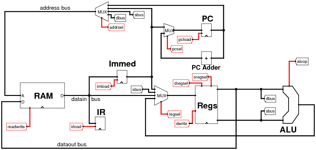
5 CPU Control Lines- Below is the main CPU diagram again, this time with the control lines shown.
- There are several 1-bit control lines:
- pcsel, increment PC or load the jump value from the Immediate Register.
- pcload, load the PC with a new value, or don't load a new value.
- irload, load the Instruction Register with a new instruction.
- imload, load the Immediate Register with a new value.
- readwrite, read from memory, or write to memory.
- dwrite, write a value back to a register, or don't write a value.
- There are also several 2-bit control lines:
- addrsel, select an address from the PC, the Immediate Register, the source register or the destination register.
- regsel, select a value to write to a register from the Immediate Register, another register, the data bus or from the ALU.
- dregsel and sregsel, select two registers whose values are sent to the ALU.
- aluop, which are the op2 bits that control the operation of the ALU.
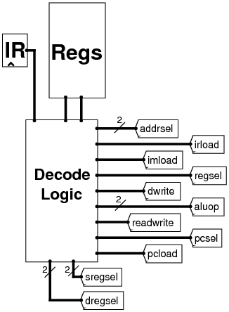
- The values for all of these control lines are generated by the Decode Logic, which gets as input the value from the Instruction Register, and the zero & negative lines of the destination register.
- It's now time to look inside the Decode Logic to see how it creates the values on the control lines.
6 Inside the Decode Logic
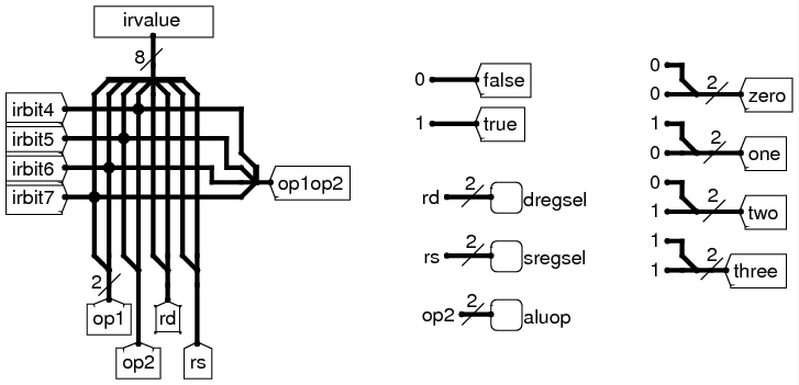
- Inside the Decode Logic block, the value from the Instruction Register is split into several individual lines irbit4, irbit5, irbit6 and irbit7. op1 and op2 are split out, with op2 exported as aluop. Finally, the 4 opcode bits from the instruction are split out as the op1op2 line.
- Several of the bits from the instruction register value are wired directly to these 2-bit outputs: dregsel, sregsel and aluop.
- The diagram looks a bit ugly as this is the way that Logisim splits groups of lines out to individual lines.
- In the Logisim implementation of the CPU, there are two 1-bit "constant" lines defined: true and false, as well as several 2-bit lines: zero, one, two and three.
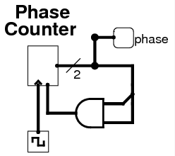
- We also need some logic to output the current phase of execution. This is done with a simple 2-bit counter which is controlled by the clock cycle, and which outputs a 2-bit phase line.
- We don't need phase 3, so the two bits of the phase line can be ANDed. When both are true, this resets the counter back to zero.
- For the rest of the decode logic, we need to look at what needs to be performed for the various phases of the CPU, and also what needs to be performed for each specific instruction.
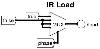
6.1 Phase Zero- On phase zero, the PC's value has to be placed on the address bus, so the addrsel line must be 0. The irload line needs to be 1 so that the IR is loaded from the datain bus. Finally, the PC must be incremented in case we need to fetch an immediate value in phase 1.
- All of this can be done using multiplexors which output different values depending on the current phase. Here is the control logic for the irload line.
- We only need to load the IR on phase 0, so we can wire true to the 0 input of the irload multiplexor, and false to the other inputs. Note: input 11 (i.e. decimal 3) to the multiplexor is never used, as we never get to phase 3, but Logisim wants all multiplexor inputs to be valid.
- Another way to look at each phase is the value which needs to be set for each control line, for each instruction.
- For phase zero, these control line values can be set for all instructions:
| op1 | op2 | instruct | pcsel | pcload | irload | imload | rw | dwrite | jumpsel | addrsel | regsel | dreg | sreg | aluop | | | xx | xx | all | 1 | 1 | 1 | 0 | 0 | 0 | 0 | 0 | x | x | x | x |
- 'x' stands for any value, i.e. accept any opcode value, output any control line value.
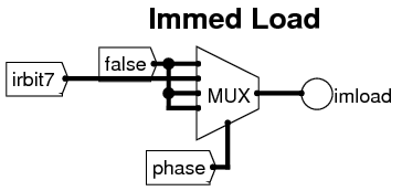
6.2 Phase One- On phase 1, we need to load the Immediate Register with a value from memory if the irbit7 from the IR is true. The PC's value has to be placed on the address bus, so the addrsel line must be 0. The imload line needs to be 1 so that the Immediate Register is loaded from the datain bus. Finally, the PC must be incremented so that we are ready to fetch the next instruction on the next phase 0.
- The imload logic is shown above. It is very similar to the irload logic, but this time an enable value is output only on phase 1, and only if the irbit7 is set.
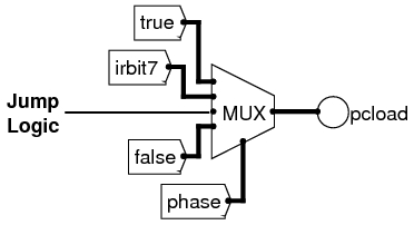
- Some of the pcload logic is shown above. The PC is always incremented at phase 0. It is incremented at phase 1 if irbit7 is set, i.e. a two-byte instruction. Finally, the PC can be loaded with an immediate value in phase 2 if we are performing a jump instruction and the jump test is true. We will come back to the jump logic later.
- We can tabulate the values of the control lines for phase 1. This time, what is output depends on the top bit of the op1 value:
| op1 | op2 | instruct | pcsel | pcload | irload | imload | rw | dwrite | jumpsel | addrsel | regsel | dreg | sreg | aluop | | | 0x | xx | all | x | 0 | 0 | 0 | 0 | 0 | 0 | 0 | x | x | x | x | | 1x | xx | all | 1 | 1 | 0 | 1 | 0 | 0 | 0 | 0 | x | x | x | x |
6.3 Phase Two- Here, the values of the control lines depend heavily on what specific instruction we are performing. Here's the table of control line outputs depending on the instruction:
| op1 | op2 | instruct | pcsel | pcload | irload | imload | rw | dwrite | addrsel | regsel | dreg | sreg | aluop | | | 00 | 00 | AND Rd, Rs | x | 0 | 0 | 0 | 0 | 1 | x | 3 | Rd | Rs | op2 | | 00 | 01 | OR Rd, Rs | x | 0 | 0 | 0 | 0 | 1 | x | 3 | Rd | Rs | op2 | | 00 | 10 | ADD Rd, Rs | x | 0 | 0 | 0 | 0 | 1 | x | 3 | Rd | Rs | op2 | | 00 | 11 | SUB Rd, Rs | x | 0 | 0 | 0 | 0 | 1 | x | 3 | Rd | Rs | op2 | | 01 | 00 | LW Rd, (Rs) | x | 0 | 0 | 0 | 0 | 1 | 2 | 2 | Rd | Rs | x | | 01 | 01 | SW Rd, (Rs) | x | 0 | 0 | 0 | 1 | 0 | 3 | x | Rd | Rs | x | | 01 | 10 | MOV Rd, Rs | x | 0 | 0 | 0 | 0 | 1 | x | 1 | Rd | Rs | x | | 01 | 11 | NOP | x | 0 | 0 | 0 | 0 | 0 | x | x | x | x | x | | 10 | 00 | JEQ Rd, immed | 0 | j | 0 | 0 | 0 | 0 | x | x | Rd | x | op2 | | 10 | 01 | JNE Rd, immed | 0 | j | 0 | 0 | 0 | 0 | x | x | Rd | x | op2 | | 10 | 10 | JGT Rd, immed | 0 | j | 0 | 0 | 0 | 0 | x | x | Rd | x | op2 | | 10 | 11 | JLT Rd, immed | 0 | j | 0 | 0 | 0 | 0 | x | x | Rd | x | op2 | | 11 | 00 | LW Rd, immed | x | 0 | 0 | 0 | 0 | 1 | 1 | 2 | Rd | x | x | | 11 | 01 | SW Rd, immed | x | 0 | 0 | 0 | 1 | 0 | 1 | x | Rd | x | x | | 11 | 10 | LI Rd, immed | x | 0 | 0 | 0 | 0 | 1 | x | 0 | Rd | x | x | | 11 | 11 | JMP immed | 0 | 1 | 0 | 0 | 0 | 0 | x | x | x | x | x |
- To make the control line logic as simple as possible, a CPU designer is always striving for regularity. However, this is often in conflict with the desired CPU functionality.
- From the table above, the ALU instructions (op1=00) and the jump instructions (op1=10) are nice and regular. All the op1=1x instructions use the Immediate Register, while the op1=0x instructions don't.
- We can always tie dregsel to Rd from the instruction, and the same goes for sregsel = Rs and aluop = op2. And irload and imload are always 0 for phase 2.
- With the remaining control lines, the regularities cease.
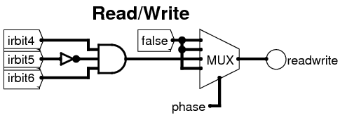
6.4 Read/Write Logic- The read/write line out to memory only needs to be enabled when we are performing SW (store word) operations, and only in phase 2.
- The op1op2 values for the two SW instructions are 0101 and 1101, so we can treat this as x101, and set readwrite true when irbit6 is on, irbit5 is off and irbit4 is on.
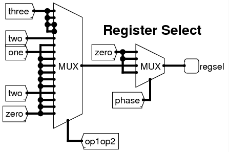
6.5 Register Select Logic- Now we get to the control lines which are messy. The first one is the regsel line, which selects the input to be written into the destination register. This can be:
| 00 (zero) | Immediate Register | | 01 (one) | sbus, i.e. the source register | | 10 (two) | datain bus | | 11 (three) | ALU output |
- Consulting the big table in the Phase Two subsection, all the ALU instructions set regsel to 3, but apart from that there is no simple logical rule to output all the possible values.
- Also, for the regsel 'x' values in the table, we can choose to output any value, as the register won't be loaded on these instructions.
- The easiest solution here is to use one multiplexor for the phase of operation, and a second multiplexor for the instruction's opcode, i.e. op1op2 is used to select the value to output.
- Each of the 16 inputs to the big multiplexor sets a regsel value for a specific instruction based on the op1op2 value, and this only gets out during phase 2. Otherwise, regsel is set to zero.
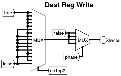
6.6 Destination Register Write Logic- Following on from regsel, we need to control dwrite, i.e. when the destination register gets written.
- This can occur only in phase 2, and again there is no simple rule that allows us to hardwire the value with simple gates: see the dwrite column in the big table above.
- Again, we can use a 16-input multiplexor, with op1op2 to choose the correct dwrite value to output on phase 2.
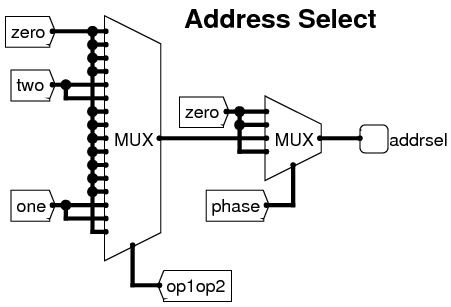
6.7 Address Select Logic- When we want to read data from main memory, the address we want to read from can be selected from these inputs:
| 00 (zero) | Program Counter | | 01 (one) | Immediate Register | | 10 (two) | sbus, i.e the source register | | 11 (three) | dbus, i.e the source register |
- The decode logic needs to output a value for addrsel which selects the correct address to assert on the address bus for each instruction during phase 0, phase 1 and phase 2.
- As with the previous two control lines, there is no simple logic to produce the value on this line based on the instruction opcode, so we resort again to a 16-input multiplexor.
- Cross-check the above logic diagram with the big table above to ensure that it will produce the right output for addrsel given the op1op2 value from the instruction.
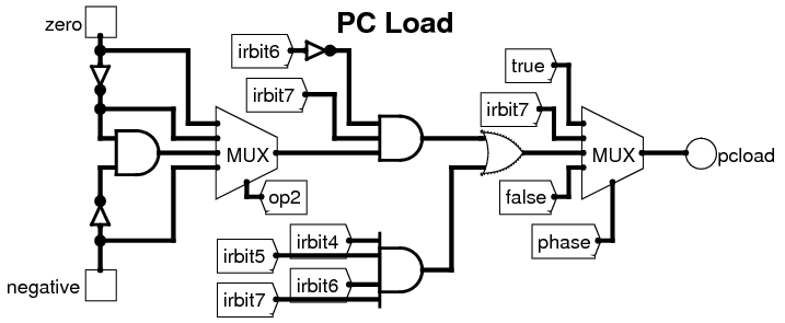
6.8 Jump Logic- We have reached the last and probably the most complicated control line in the CPU, pcload, which determines when the Program Counter is updated.
- Actually, it's not that complicated, it just looks ugly. You have seen the logic for phase 0 and phase 1. Now we need to look at the logic for the jump instructions.
- One of the jump instructions, op1op2 = 1111, always sets the PC to the Immediate Register.
- The other jump instructions only set PC to Immediate Register when a specific test is true:
| op1op2 | Test | Zero | Negative | | | 1000 (JEQ) | Rd == 0 | 1 | x | | 1001 (JNE) | Rd != 0 | 0 | x | | 1010 (JGT) | Rd > 0 | 0 | 0 | | 1011 (JLT) | Rd < 0 | x | 1 |
- Here is the logic to set pcload for all phases:
- The OR gate which connects to the phase 2 input of the right-hand multiplexor chooses either a successful jump test (top-left input) OR a "jump always" instruction (bottom-right input).
- The "jump always" instruction is op1op2 = 1111, so a 4-input AND gate is used to select for only this opcode.
- The left-hand multiplexor outputs true when the EQ/NE/GT/LT decision is true, for any instruction (not just a jump instruction). Compare the gate logic here with the truth table above.
- But we must make sure that we only output the EQ/NE/GT/LT decision on jump instructions, i.e. when op1op2 = 10xx. Thus we use the 3-way AND gate and also use the irbit6 and irbit7 lines as inputs.
6.9 Finally ...- Putting this all back together, we now have this device:
which controls the dataflow for the whole CPU:
7 Implementing the CPU- Here are the Logisim implementation files for the CPU, along with the memory image for the program in the following section.
- CPU.circ
- ALU.circ
- cpumem.img
- Download all three into the same folder.
- Run Logisim, and open the CPU.circ file. You will see the CPU, but there are extra displays that show the values in the registers and on some of the datapaths and control lines.
- To load the RAM with the memory image, right-click on the RAM device, choose Load Image, navigate to the cpumem.img file, then click on OK.
- To run the program, type control-T repeatedly. Each control-T performs half of one clock cycle.
8 An Example Program- It's time to see an example program written for this CPU.
- In memory starting at location 0x80 is a list of 8-bit numbers; the last number in the list is 0.
- We want a program to sum the numbers, store the result into memory location 0x40, and loop indefinitely after that.
- We have 4 registers to use. They are allocated as follows:
- R0 holds the pointer to the next number to add.
- R1 holds the running sum.
- R2 holds the next number to add to the running sum.
- R3 is used as a temporary register.
- Here is the assembly-style code for the program.
LI R1,0x00 # Set running sum to zero LI R0,0x80 # Start at beginning of list loop: LW R2, (R0) # Get the next number JEQ R2, end # Exit loop if number == 0 ADD R1, R2 # Add number to running sum LI R3, 0x01 # Put 1 into R3, so we can do ADD R0, R3 # R0++ JMP loop # Loop back end: SW R1, 0x40 # Store result at address 0x40 inf: JMP inf # Infinite loop - Converting to machine code, here are the hex values to put into memory starting at location 0:
| LI R1,0x00 | e4 00 | | LI R0,0x80 | e0 80 | | LW R2, (R0) | 48 | | JEQ R2, end | 88 0d | | ADD R1, R2 | 26 | | LI R3, 0x01 | ec 01 | | ADD R0, R3 | 23 | | JMP loop | ff 04 | | SW R1, 0x40 | d4 40 | | JMP inf | ff 0f |
- With the CPU loaded up into Logisim, and the memory loaded with the above data values, we can start the program running.
- Watch the phases of operation. Watch the IR get loaded with an instruction.
- Watch the Immediate Register get loaded with a value.
- On the LW instruction, watch as the sbus value is selected to be placed on the address bus, and the datain value is written to the destination register.
- On ALU instructions, watch the sbus and dbus values, the aluop, and the result which is written back into the destination register.
- On the JEQ instruction, watch the value of N and Z into the Decode Logic, and the resulting pcsel and pcload values.
9 Other Areas of the CPU- This last section covers the remaining parts of the CPU. We probably won't have time in the tutorial to explore these areas, but they are documented here anyway.
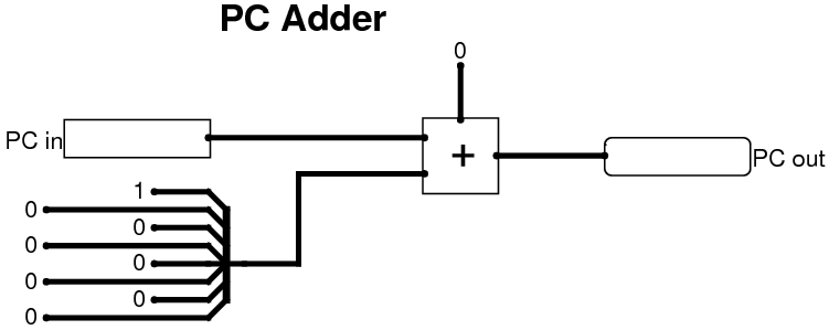
9.1 The PC Adder- The PC Adder logic is nice and simple.
- Using the built-in Logisim adder unit, take the old PC value as one input, and the 8-bit constant 00000001 as the other input, add them together, and output the new PC value.
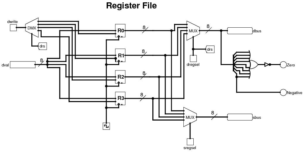
9.2 The Register File- The logic for the register file looks ugly, so we will look at each section in turn.
- In the middle are the four registers, which are built-in Logisim units.
- Each register's value is sent to two multiplexors on the right.
- The top multiplexor selects one of the register values based on the dregsel control line, and thus outputs one value on the dbus line to the ALU.
- Similarly, the bottom multiplexor selects one of the register values based on the sregsel control line, and thus outputs one value on the sbus line to the ALU.
- There is also logic to test if the dbus value is negative. The eight bits on the dbus are split out, and the most significant bit is the Negative output. This implies that we use twos-complement representation for signed values.
- All eight bits of the dbus are ORed together and then negated.
- When the dbus is zero, all bits are zero. The OR output is zero, and thus the negated output on the Zero line is true.
- On the left, each register takes three inputs:
- a value to possibly load. All registers are hard-wired to the input dval which holds the value to load.
- the clock pulse, which tells the registers when to load.
- a write enable signal. Only when the write enable signal is 1 can a register overwrite its old value.
- The demultiplexor at the top-left takes as input dwrite (i.e. the write signal), and based on the dreg value, selects which register to send the dwrite signal to. All other registers will get a write signal of 0, i.e. not to perform a write operation.
|
|
 /1
/1 

 eetop公众号
 创芯大讲堂
创芯大讲堂
 创芯人才网
创芯人才网

 创芯人才网
创芯人才网
 IP卡
IP卡 狗仔卡
狗仔卡 发表于 2013-5-21 19:15:19
 提升卡
提升卡 沉默卡
沉默卡 喧嚣卡
喧嚣卡 变色卡
变色卡